Optical Microscopy versus Scanning Electron Microscopy in Medical Device Testing
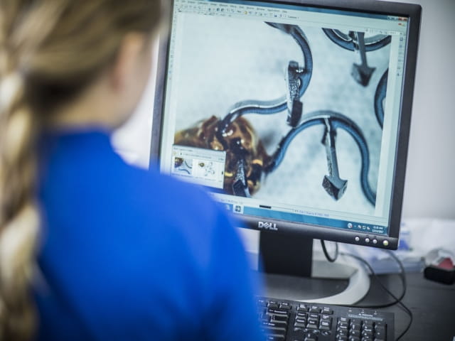
Optical Microscopy and Scanning Electron Microscopy are fundamental inspection methods in the medical device industry, and each has unique benefits and capabilities.
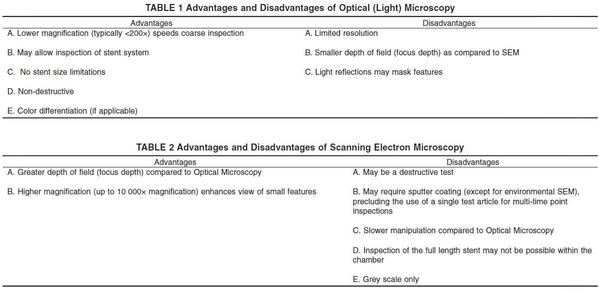
The main difference between a Scanning Electron Microscope (SEM) and an Optical Microscope (OM) is the type of beam applied to the sample. For optical microscopy, a beam of light is applied, allowing the observer to analyze the effects of light as it interacts with the sample. In contrast, scanning electron microscopy uses a beam of electrons to examine the sample, allowing the observer to analyze the effects of electrons as they interact with the material.
Advantages and Disadvantages
Optical microscopy is an ideal method for general inspection purposes, but scanning electron microscopy can provide the user with incredibly detailed topographical and compositional information. A scanning electron microscope typically features three types of detectors: a Secondary Electron Detector (SED), a Back-Scattered Electron Detector (BSED), and an Energy Dispersive Spectrum Detector (EDS).
The SED provides detailed topographical information to the user since secondary electrons interact primarily with the sample surface and have a large reflection angle, while the BSED provides both basic topographical and basic compositional information to the user since back-scattered electrons penetrate further into the material, and have a smaller reflection angle. The compositional data is relative – low-atomic-number materials appear dark and high-atomic number materials appear light in the SEM, but the exact chemical composition cannot be provided by the BSED.

EDS提供详细的化学成分信息。在某些情况下,使用扫描电子显微镜作为二次检查方法是有益的。首先,光学显微镜用于观察总缺陷。可以使用这种方法轻松操纵样本,并且可以相对较快地绘制和记录所有总缺陷以进行进一步审查。接下来,扫描电子显微镜用于更详细地观察图表的总缺陷,并观察光学显微镜未见的微缺陷。这种两相方法结合了与每种检查方法相关的益处,并在更少的时间内提供更详细的检查(与仅限SEM的全面检查相比)。
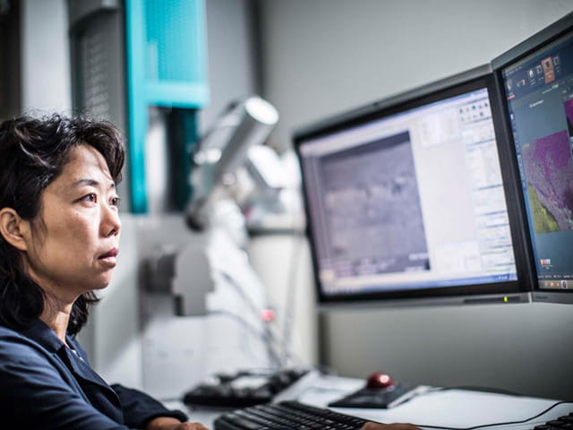
Element has an Aspex Model 3025 SEM system with Automated Feature Analysis (AFA) Software and EDS (Energy Dispersive Spectrum) capabilities. The system is used for the inspection of defects on medical devices as well as particulate analysis studies. For the later, particulates shed from the device are captured on gold or carbon plated filters and up to 6 filters are placed in the SEM for subsequent analysis. The AFA software analyzes each filter individually and gathers a considerable amount of data on each particle.
Conclusions
Optical Microscopy and Scanning Electron Microscopy are fundamental inspection methods in the medical device industry, and Element offers both capabilities. Each has advantages and disadvantages, and our test engineers will help you determine which is most appropriate for your test needs. When combined with our extensive testing knowledge, you can feel confident that the inspection data provided by Element is the best available in the industry.
通过介绍与您的相关文章爱游戏ayx开户


